
Timing is key to boil eggs just how you like them. This designed implemented on a FPGA can set a timer to alert you when your eggs are ready. The design has pre-set timers for soft, medium, or hard-boiled eggs. Any time can be set with the push buttons for other timed tasks. Simple logic implementation using FPGA.
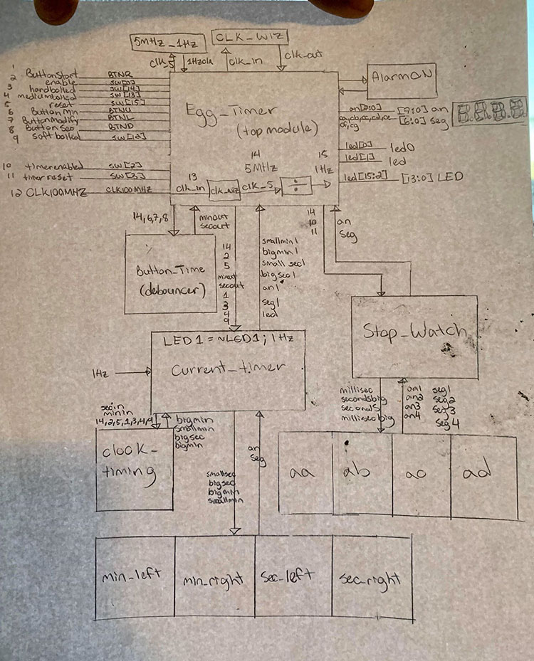
Due to restrictions in Vivado 2016.3, it was not possible to install the Nexys4 DDR board. Consequently, a fully wired and correct Box Diagram could not be produced. Instead, I provided the schematic of the design using a similar part, supplemented with a hand-drawn Box Diagram.
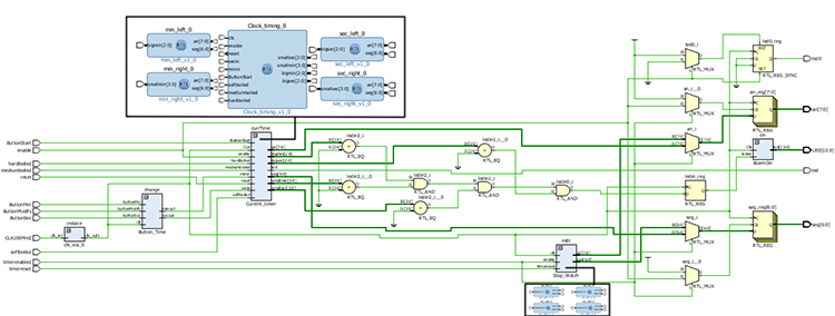
The design primarily serves as a timer that counts down from a preset or chosen time to zero, displayed on a seven-segment anode. Two key modules, ButtonTime (debouncer) and Current-timer (counter, timer, display, 7segment), work together to accomplish this. Additional features include a switch-enabled stopwatch, time presets, and a visual LED display to signal zero time. The entire design is synchronous, leveraging the on-board clock (100MHz) divided to 5MHz via the Clock Wizard IP, and further divided to 1Hz by another divider module (5MHz1Hz).
The Verilog code for this project is available on my GitHub here.
The design underwent rigorous testing and simulation using a custom-made test bench to ensure it functions as expected even without using an FPGA.
The test bench code can be found on my GitHub here.
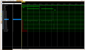
Figure 1: tb_egg Behaviour Simulation

Table 1: Post-Synthesis Resource Utilization
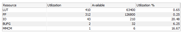
Table 2: Post-Implementation Resource Utilization
The Clocking Wizard IP can only produce a clock as low as 5MHz. In this project, using the same clock divider module twice to produce a 1Hz clock proved more practical. While if else chains are easy to code, they tend to be resource-intensive compared to behavioral code.
…return to projects.ibrahimsaid.ca or ibrahimsaid.ca.